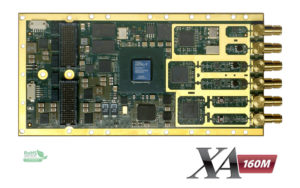
XA Artix7 FPGA Series
Audio to 500MSPS.
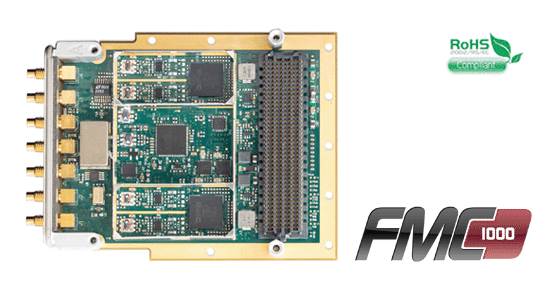
FMC Series
250MSPS to 1000MSPS.
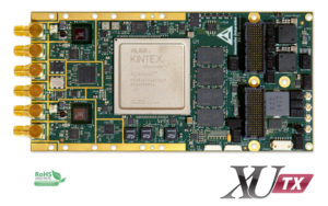
Kintex Ultrascale XMC Series
2GSPS to 5.1GSPS.
ePC-K7
Hosts for FMC modules
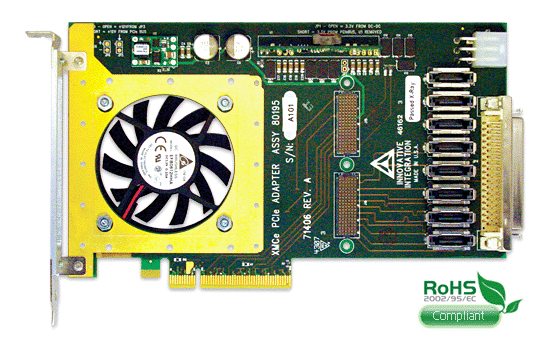
XMC to PCIe
Adapters for PMC & XMC modules