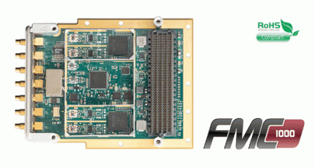
Features
- Two A/D inputs
- 1000 MSPS, 14-bit (1250 MSPS version coming soon)
- 4 DDC’s in AD9680, with NCO and decimation x2, x4, x8, x16.
- AC or DC coupled
- Two D/A Outputs
- 1000 MSPS, 16-bit D/A
- Dac has 1x-16x interpolation and NCO
- AC or DC coupled
- Sample clocks and timing and controls
- External clock/reference input
- Programmable PLL
- 10 MHz, 0.5 ppm reference
- Integrated with FMC triggers
- FMC module, VITA 57.1
- High Pin Count
- Compatible with 1.2 to 3.3V VADJ
- Power monitor and controls
- 6W typical (AC-coupled inputs)
- Conduction Cooling per VITA 20 subset
- Environmental ratings for -40 to 85C, 9g RMS sine, 0.1g2/Hz random vibration
Applications
- Waveform Generation
- Wireless Receiver and Transmitter
- RADAR
- Medical Imaging
- High Speed Data Recording and Playback
- IP development
Overview
The FMC-1000 is a high speed digitizing and signal generation FMC I/O module featuring two, 1000 MSPS A/D channels and two 1000 MSPS D/A channels supported by sample clock and triggering features.
The FMC-1000 incorporates two AD9680, 14-bit 1000 MSPS A/Ds, plus a dual channel, 1000 MSPS update rate DAC38J82 DAC. Analog I/O may be either AC or DC coupled. Receiver IF frequencies of up to 1000 MHz are supported. The sample clock is from either an ultra-low- jitter PLL or external input. Multiple cards can be synchronized for sampling.
The FMC-1000 power consumption is 6W for typical operation. The module may be conduction cooled using VITA20 standard and a heat spreading plate. Ruggedization levels for wide-temperature operation from -40 to +85C operation and 0.1 g2/Hz vibration. Conformal coating is available.
Support logic in VHDL is provided for integration with FPGA carrier cards. Specific support for Innovative carrier cards includes integration with Framework Logic tools that support VHDL/Verilog and Matlab developers. The Matlab BSP supports real-time hardware-in-the-loop development using the graphical block diagram Simulink environment with Xilinx System Generator for the FMC integrated with the FPGA carrier card.
Software tools for Innovative carrier cards include host development include C++ libraries and drivers for Windows and Linux. Application examples demonstrating the module features are provided.
Dataflow
The FMC modules come with logic to use them on the Innovative FMC hosts (ePC-K7, mini-K7 & others). The logic includes a sample streaming interface to the system processor. Please see the data flow diagram for the generic model.
The simplied data flow from Adc(s) to host application works as follows. Samples from the Adc(s) are clocked into the FPGA. The samples are packed where necessary for efficient use of the RAM chips. The RAM is used as a virtual FIFO to decouple the continuous stream of the Adc(s) from the block transfer nature of PCIe. The user application sets the packetsize. When a whole packet of data is available in the RAM, the PCIe DMA controller does a bus master transfer to the host memory. At configuration time the device drivers reserve physical memory for this purpose. When the transfer is complete, the DMA controller sends an interrupt to Malibu which then copies the packet from the busmaster area to virtual memory and then fires an event in the User application with a reference to the data.
The FMC host memory is usually 256MB or more. If the host can not consume the data as fast as the Adc(s) produces it, the memory fills with samples. This defines the longest continuous capture length possible.
The simplified data flow in the reverse direction for host to Dac(s) is similar. Onboard RAM is configured as a virtual FIFO between the PCIe and the Dac(s). When there is room in the RAM chips for a packet of samples, the PCIe DMA controller interrupts the host, which then signals the application to provide a packet of samples. The samples are copied from virtual memory to physical memory and then the PCIe DMA controller copies them into RAM. As data is flowed to the DAC(s) the RAM has more space for more packets and so the process is repeated.


