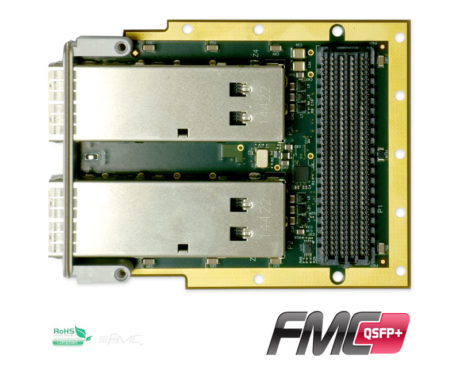
Features
- Two QSFP+ ports
- Up to 40 Gbps per port (IEEE 802.3ba)
- 2-wire I2C communication interface and other low-speed electrical interface compliant to SFF 8436 and QSFP Multisource Agreement (MSA)
- Programmable low jitter clock supports 0.16 to 350 MHz range with 1PPM step
- Spread-spectrum clock support
- 10 MHz, 0.5 PPM reference
- FMC (ANSI/VITA57) Module (Note: module extends beyond FMC form-factor on the face plate. See mechanical requirements.)
Applications
- Remote Radio Head receiver
- OBSAI and CPRI interface
- Serial FPDP and SRIO fiber optic ports
Chipset
- Analogue to Digital Converter(s) = N/A
- FPGA = None, on host board
- Digital to Analogue = N/A
Chipset
FMC-QSFP+ provides two QSFP+ ports on a standard FMC module with programmable clock and support features. Fiber optic links to remote IO, such as Remote Radio Head applications, from host processing and FPGA cards support up to 40 Gbps bit rates.
The QSFP+ ports are compatible with SFF-8436 transceivers, supporting both copper and fiber optic links. The two ports are fully independent on the module. QSFP+ control and monitoring signals are mapped to the FMC interface for I2C control port, power mode, reset, presence of cable, and Interrupt events.
A flexible reference clock for on the FMC-QSFP+ is fully programmable over the 0.16 to 350 MHz range. The clock can be programmed for all common rates for standards such as OC-12, OBSAI, CPRI, GbE, sFPDP and SONET. The clock has jitter performance of less than 1 ps RMS max, allowing it to meet the most stringent requirements for these applications. An on-card 10MHz Oscillator with 0.5 PPM stability is used as the PLL reference.
The FMC-QSFP+ is fully electrically compatible with FMC (ANSI/VITA 57) specifications for IO module. Mechanically, the module will fit FMC sites, however the QSFP+ connectors protrude slightly past the face of the bezel. The module is compatible with FMC HPC sites. The module consumes <750 mW exclusive of QSFP+ modules.
The FMC is provided with VHDL code illustrating the interfaces. Specific FPGA and platform support is provided for Innovative’s VPX- COP and PEX-COP FPGA cards.
Software libraries and examples for C++ host development are provided. Application examples demonstrating the module features are provided for Innovative Integration platforms in for Windows, Linux and VxWorks.
Dataflow
The FMC modules come with logic to use them on the Innovative FMC hosts (ePC-K7, mini-K7 & others). The logic includes a sample streaming interface to the system processor. Please see the data flow diagram for the generic model.
The simplied data flow from Adc(s) to host application works as follows. Samples from the Adc(s) are clocked into the FPGA. The samples are packed where necessary for efficient use of the RAM chips. The RAM is used as a virtual FIFO to decouple the continuous stream of the Adc(s) from the block transfer nature of PCIe. The user application sets the packetsize. When a whole packet of data is available in the RAM, the PCIe DMA controller does a bus master transfer to the host memory. At configuration time the device drivers reserve physical memory for this purpose. When the transfer is complete, the DMA controller sends an interrupt to Malibu which then copies the packet from the busmaster area to virtual memory and then fires an event in the User application with a reference to the data.
The FMC host memory is usually 256MB or more. If the host can not consume the data as fast as the Adc(s) produces it, the memory fills with samples. This defines the longest continuous capture length possible.
The simplified data flow in the reverse direction for host to Dac(s) is similar. Onboard RAM is configured as a virtual FIFO between the PCIe and the Dac(s). When there is room in the RAM chips for a packet of samples, the PCIe DMA controller interrupts the host, which then signals the application to provide a packet of samples. The samples are copied from virtual memory to physical memory and then the PCIe DMA controller copies them into RAM. As data is flowed to the DAC(s) the RAM has more space for more packets and so the process is repeated.


