
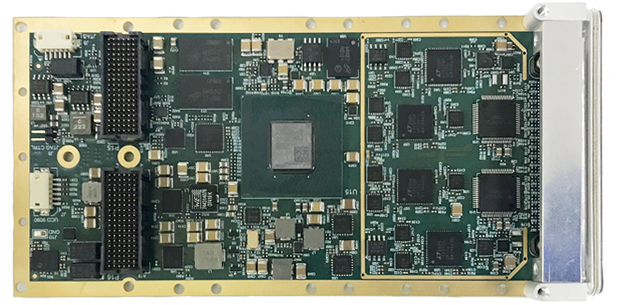
PCIe XMC Servo Module – Sixteen channel 500 ksps 16 bit Adc, sixteen channel 2.5 MSPS 16 bit Dac, Xilinx Artix-7 FPGA, PLL, 4 lane PCIe and 1 GB DDR3 Memory


Related products
Features
- 16x 18-bit simultaneously sampling 500 kSPS A/D channels
- Two programmable Input Ranges (+/-5V and +/-10V) with Remote Ground Sensing
- 1 MO Input Impedance
- Overvoltage Input Clamp With 9-kV ESD
- DNL: ±0.5 LSB typ.; INL: ±2.0 LSB typ.
- SNR: 94 dB typ.; THD: -109 dB typ.
- On-Chip Digital Filter for Oversampling (OS)
- 24 kHz typ. 3 dB Bandwidth (±10-V Input, no OS)
- 16x 16-bit up to 2.5 MSPS D/A channels with 6 software programmable Output Ranges:
- Unipolar: 0V to 5V, 0V to 10V
- Bipolar: ±2.5V, ±5V, ±10V, –2.5V to 7.5V
- 4µs Settling Time to ±1 LSB
- +/-10 mA min Load Current
- Output Short Current protection
- 50 O Output Impedance
- DIO on P16 (19 differential pairs)
- Xilinx Artix-7 FPGA
- DDR3 Memory
- Precision on-board programmable or external reference clock
- Synchronized system sampling using common reference clock and triggers
- 1 PPS and Sync Inputs
- Framed, software or external triggering
- Log acquisition timing and events
- Power management features
- PCI Express 2.0 XMC Module (75×150 mm)
- Use in any PCI Express desktop, compact PCI/PXI, PXIe, or cabled PCI Express
- Drivers for Windows, Ubuntu (NVidia Xavier, TX2), Centos
Applications
- Industrial Automation and Controls
- Multichannel Data Acquisition Systems
- Scientific and Industrial equipment
- Test and Measurement
Useful resources on Youtube
These videos may be helpful in learning about using the FPGA on this board.
Overview
Servo Loops
The XA-Servo is an XMC IO module featuring sixteen 18-bit, up to 500kSPS high-precision SAR A/D channels with high input impedance and remote ground sensing and sixteen 16-bit up to 2.5MSPS D/A channels with 4µs settling time, +/- 10mA guaranteed output current designed for industrial, scientific, control, test and measurement applications.
Flexible trigger methods include counted frames, software triggering and external triggering. The sample rate clock is either an external clock or onboard programmable precision clock source.
Data acquisition control, signal processing, buffering, and system interface functions are implemented in a Xilinx Artix-7 FPGA device.
Artix-7 FPGA
Two 256Mb x16 DDR3 type memories provide data buffering and FPGA computing memory. The logic can be fully customized using VHDL and the FrameWork Logic toolset. The PCI Express 2.0 interface supports data rates up to 1600 MB/s for unbuffered continuous data or burst data streams. When using a standard configuration involving DDR3 buffered data, a continuous data rate up to 1300 MB/s is supported.
19 Differential (LVDS) Digital IO (DIO) Pairs along with 4 pairs of RX/TX high-speed Serial Link lanes are available on the XMC P16 connector.
NVIDIA® Jetson GPU
The XA-Servo software support now includes drivers for development on the NVIDIA® Jetson TX2 GPU platform and the XVIDIA® Xavier that are aimed at Artificial Intelligence and is being increasing used in Photonics and Distributed Acoustic Sensing applications.
Dataflow
The board comes complete with working logic (Framework Logic) and software drivers (Malibu). Please see the data flow diagram.
The simplied data flow from Adc(s) to host application works as follows. Samples from the Adc(s) are clocked into the FPGA. The samples are packed where necessary for efficient use of the RAM chips. The RAM is used as a virtual FIFO to decouple the continuous stream of the Adc(s) from the block transfer nature of PCIe. The user application sets the packetsize. When a whole packet of data is available in the RAM, the PCIe DMA controller does a bus master transfer to the host memory. At configuration time the device drivers reserve physical memory for this purpose. When the transfer is complete, the DMA controller sends an interrupt to Malibu which then copies the packet from the busmaster area to virtual memory and then fires an event in the User application with a reference to the data.
The simplified data flow in the reverse direction for host to Dac(s) is similar. Onboard RAM is configured as a virtual FIFO between the PCIe and the Dac(s). When there is room in the RAM chips for a packet of samples, the PCIe DMA controller interrupts the host, which then signals the application to provide a packet of samples. The samples are copied from virtual memory to physical memory and then the PCIe DMA controller copies them into RAM. As data is flowed to the DAC(s) the RAM has more space for more packets and so the process is repeated.
On XU-RT the Adc memory is 2GB and the Dac memory is 2GB.
Support
The product comes with the following support items to help you with your project:
- Malibu Software, including
- Arb, Snap, Wave & Stream – example applications as sourcecode to setup the board for acquisition and waveform generation. Shows designer how to stream Adc samples to host file and stream from host to Dacs, written in C++.
- Drivers for Windows/Linux, 32 and 64 bit.
- Framework logic (source is extra cost)
- Makes the XU board act as a data acquisition card, using onboard DDR as huge virtual FIFO’s.
- iiForum
- Knowledgebase of previous users of the XMC board.
- Access to the XMC engineers.
- Full hardware, software and firmware manuals as PDF.
- Telephone/email technical support from EnTegra Solutions and Innovative Integration.