Features
- Kintex7 FPGA board with FMC site
- Desktop/Server 3/4 full-length FPGA Coprocessor Card
- FMC HPC I/O site (VITA 57) with x8 10.0 Gbps MGT lanes, 80 LVDS pairs (LA, HA, HB full support)
- FPGA Computing Core
- Xilinx Kintex-7 K325 or K410
- Single Bank 256Mb x 64 DDR3 (2048MB total)
- 256Mb BPI Configuration FLASH
- External clock input
- External trigger input supports multi-card synchronization and coordinated sampling
- 1 PPS Input
- 8 lane PCIe Express Gen 2 interface providing 4 GB/s burst and 3.2 GB/s sustained transfer rates
- On-board USB to JTAG programmer allows FPGA programming without external hardware
- 14-pin JTAG header with Xilinx compatible pinout
- < 15W typical power excluding FMC
- x4 Secondary Port usable as PCI Express or Aurora
- <15W typical excluding FMC
- Temperature and power monitoring
Chipset
- Analogue to Digital Converter(s) = N/A (use FMC site)
- FPGA = Xilinx Kintex 7 325T2/410T2 FPGAs
- Digital to Analogue = N/A (use FMC site)
Overview
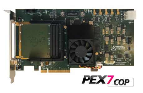
The PEX7-COP is a flexible FPGA co-processor card that integrates a Kintex-7 FPGA computing core with an industry-standard FMC I/O module on a three-quarter-length PCI Express desktop or server card.
The FPGA computing core features the Xilinx Kintex-7 FPGA family and is offered in two densities, K325 or K410. The K410 FPGA provides over 2000 DSP MAC elements operating at up to 500 MHz. The FPGA core has a 2048 MB DDR3 DRAM bank attached.
For system communications, the PEX7-COP utilizes a PCI Express x8 Gen2 port capable of up to 3.2 GB/s sustained operation with 4 GB/s burst rate.
An FMC site, conforming to VITA 57 standard, provides configurable I/O for the PEX7-COP. The FMC site has full support for the high pin count connector (HPC), with 80 LVDS pairs and 8 high-speed lanes (TX/RX) at up to 10 Gbps per lane directly connected to the FPGA. The FMC site is readily adapted to application-specific custom modules.
The FPGA logic can be fully customized using the Frame Work Logic tool set. The toolset provides support for both MATLAB and RTL designs. The MATLAB BSP supports real-time hardware-in-the-loop development using the graphical, block diagram Simulink environment with Xilinx System Generator. IP cores for a range of signal processing cores for applications such as wireless, RADAR and SIGINT such as DDC, demodulation, and FFT are also available.
Software tools for host development include C++ libraries and drivers for Windows and Linux (including real-time variants). Application examples demonstrating the module features are provided.
The HPC FMC site can host the FMC-250, FMC-310, FMC-500, FMC-1000, FMC-Servo, FMC-SDF or the FMC-SFP+.
Dataflow
The board comes complete with working logic (Framework Logic) and software drivers (Malibu). Please see the data flow diagram.
The simplied data flow from Adc(s) to host application works as follows. Samples from the Adc(s) are clocked into the FPGA. The samples are packed where necessary for efficient use of the RAM chips. The RAM is used as a virtual FIFO to decouple the continuous stream of the Adc(s) from the block transfer nature of PCIe. The user application sets the packetsize. When a whole packet of data is available in the RAM, the PCIe DMA controller does a bus master transfer to the host memory. At configuration time the device drivers reserve physical memory for this purpose. When the transfer is complete, the DMA controller sends an interrupt to Malibu which then copies the packet from the busmaster area to virtual memory and then fires an event in the User application with a reference to the data.
On PEX7-COP the Adc memory is 1GB.
The simplified data flow in the reverse direction for host to Dac(s) is similar. Onboard RAM is configured as a virtual FIFO between the PCIe and the Dac(s). When there is room in the RAM chips for a packet of samples, the PCIe DMA controller interrupts the host, which then signals the application to provide a packet of samples. The samples are copied from virtual memory to physical memory and then the PCIe DMA controller copies them into RAM. As data is flowed to the DAC(s) the RAM has more space for more packets and so the process is repeated.
On PEX7-COP the Dac memory is 1GB.
Applications
- FPGA co-processing and acceleration
- Wireless Receivers – LTE, WiMAX, SATCOM
- RADAR, Signal Intelligence
- Medical Imaging
- High Speed Data Recording and Playback
- IP development
Content on Youtube
This videos may be helpful in learning about using the FPGA on this board.


